Collaborate. Create. Solve.

Latest Project Activity
New Project Launch
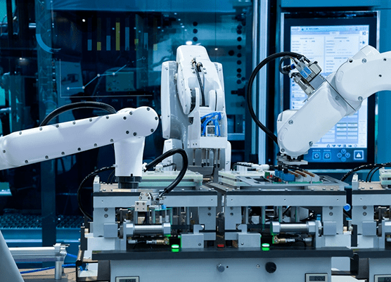
HDP has done extensive work on evaluating Pb-free solder joint reliability. These evaluations most often have used OSP on the test vehicles to provide a consistent baseline for evaluations. Most of the projects have used the same set of devices and PCB test vehicle over this period.
PCB final finishes may include Au, Ni, Pd and Ag for high performance applications. Two HDP final finish projects were completed in 2025:
• Final Finish Layer Deposits for High Frequency
• Single Surface Finish for Soldered & Compression Contact Pads, Phase 2
• Single Surface Finish for Soldered & Compression Contact Pads, Phase 2
The hypothesis is that small additions of final finish metals do not alter the composition or microstructure enough to alter the failure mode and degrade solder joint reliability. There is evidence that some final finishes can cause failures by mechanisms other than by wear-out solder fatigue. However, because non-wear-out failures in reliability testing can confound data interpretation, objective data does not exist to prove the hypothesis.
This project proposes using accelerated temperature cycling with a single Pb-free solder alloy and several finishes to generate reliability data. The final finishes to be used will be informed by the recently completed projects with the project team making a final determination of scope. SAC 305 is proposed as the Pb-free solder to be used. OSP will be used as a benchmark. The objective is to determine the rank order of final finish performance with the same test vehicle used in previous solder joint reliability projects.
The expected benefits of this project are:
• Generate data to understand the impact of final finishes on solder joint reliability.
• Test the hypothesis that final finishes do not impact Pb-free solder joint reliability in thermal cycling.
• Test the hypothesis that final finishes do not impact Pb-free solder joint reliability in thermal cycling.
About Us
Save The Date—2026 Member Meetings
The HDP Annual Member Meeting, hosted by UL Solutions, was held on March 4-5 in San Jose, California. The meeting was well attended with active member participation in presentations and discussions. We look forward to equally successful meetings in the Spring and Fall:
Spring Meeting
• When: June 3-4
• Where: Bangkok, Thailand
• Host: Sundell
Fall Meeting
• When: October 21-22
• Where: Rochester, Minnesota
• Host: IBM
